200mm vs 300mm Silicon Wafers
More from the Category
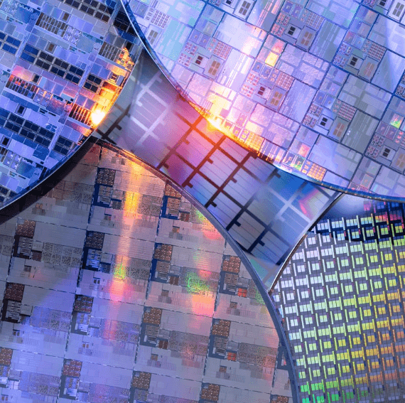
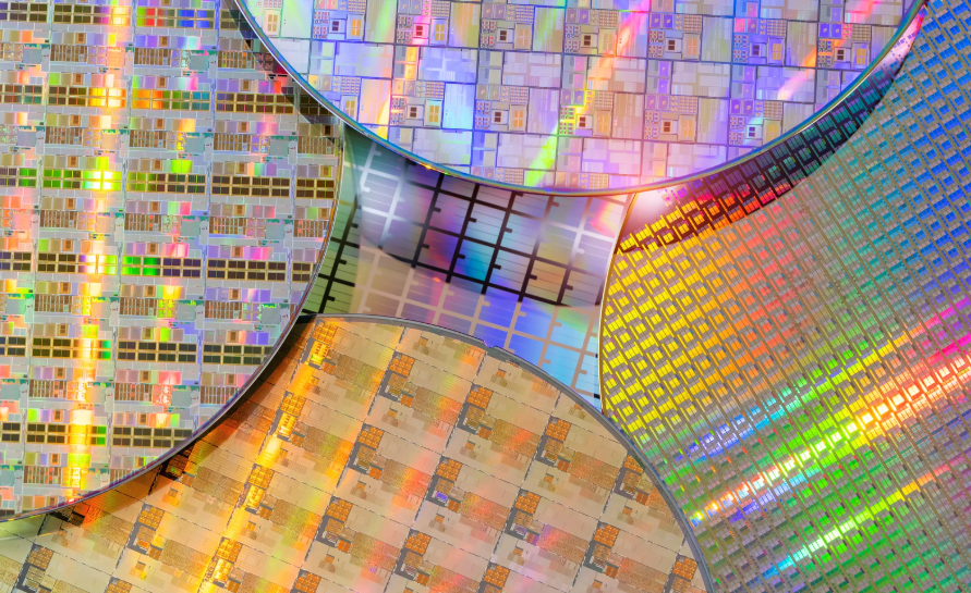
Every microprocessor, memory chip, and integrated circuit begins as a thin slice of ultra-pure silicon. As demand for faster, more efficient, and cost-effective chips grows, so does the need for larger and more advanced silicon wafer sizes.
For years, the industry has relied on 200mm and 300mm wafers as the standard for chip production. These two sizes dominate semiconductor fabrication, but they serve different purposes in the supply chain. The debate over 200mm vs 300mm wafer technology isn’t just about dimensions—it’s about efficiency, cost, and the evolving needs of semiconductor manufacturers.
The shift from 200mm to 300mm wafers has been driven by the need to reduce manufacturing costs while increasing chip output. Larger wafers mean more chips per wafer, which improves economies of scale. However, the transition is not always straightforward. While 300mm wafer production is standard for high-volume, cutting-edge semiconductors, 200mm wafers remain essential for legacy processes, power devices, and specialized applications.
This article explores the differences between 200mm and 300mm wafers, their impact on semiconductor production, and the economic and technological factors driving the industry’s wafer size choices.
Evolution of Silicon Wafer Sizes
Silicon wafer sizes have steadily increased over the decades, driven by the need for more efficient semiconductor manufacturing. In the early days of chip production, wafers were as small as 50mm in diameter. As technology advanced, wafer sizes grew to 100mm, then 150mm, and eventually 200mm, which became the industry standard in the 1990s.
The introduction of 300mm wafers in the early 2000s marked a significant shift. These larger wafers offered manufacturers a way to produce more chips per wafer while reducing overall production costs. The move from 200mm to 300mm wafers required substantial investments in new fabrication equipment and facilities, but the long-term economic benefits made it worthwhile for high-volume production.
The motivation for increasing wafer sizes has always been the same: efficiency. A larger wafer provides more usable surface area, which allows manufacturers to produce more chips per production cycle. This not only reduces costs per chip but also improves yield, as modern lithography techniques can make better use of the available silicon.
Despite the advantages of larger wafers, 200mm technology remains widely used. Many older fabrication plants still rely on 200mm wafer processes for power electronics, sensors, and analog devices. Expanding beyond 300mm has been explored, with experimental 450mm wafers tested in research settings, but the cost and complexity of upgrading manufacturing lines have slowed widespread adoption.
As the semiconductor industry continues to grow, the balance between 200mm and 300mm wafer production will be shaped by both technological advancements and economic realities.
Key Differences Between 200mm and 300mm Wafers
The transition from 200mm to 300mm wafers was not just about size — it introduced significant changes in manufacturing efficiency, cost structure, and application areas. While both wafer sizes are still widely used, their differences shape how semiconductor companies approach production.
Size and Surface Area
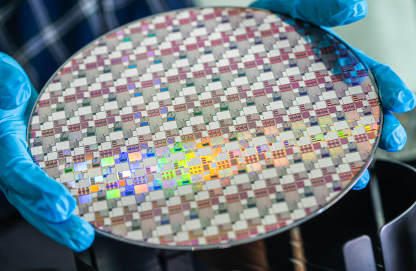
The most obvious difference is the diameter. A 200mm wafer has a surface area of about 31,400 square millimeters, while a 300mm wafer provides nearly 70,700 square millimeters. This increase more than doubles the available space for fabricating chips, which means manufacturers can produce more dies per wafer.
The ability to fit more integrated circuits onto a single wafer reduces the cost per chip, making 300mm wafers the preferred choice for high-volume production, particularly for processors, memory chips, and advanced logic devices.
Manufacturing Efficiency
Larger wafers improve efficiency, but they also require more advanced fabrication technology. The move from 200mm to 300mm introduced more automation, reducing the reliance on manual handling and increasing production yields. Automated wafer transport and processing systems minimize contamination and defects, further improving efficiency.
However, the transition to 300mm required substantial investment in new fabrication tools, which made it impractical for some manufacturers to upgrade. Many existing fabs optimized for 200mm production continue to operate, especially in areas where upgrading is cost-prohibitive or unnecessary.
Technological Applications
The differences in wafer size also dictate their application in the semiconductor industry.
● 200mm wafers are widely used in the production of analog devices, power semiconductors, MEMS (microelectromechanical systems), and specialty chips. These applications do not always benefit from the high chip density of 300mm wafers, making 200mm fabs viable for decades.
● 300mm wafers dominate in the production of high-performance computing chips, DRAM, NAND flash memory, and advanced logic devices. Their efficiency and cost advantages make them the standard for the most cutting-edge semiconductor processes.
While 300mm wafer production is now the norm for high-end semiconductor manufacturing, demand for 200mm wafers remains strong, particularly in industries that rely on legacy nodes.
Economic Considerations
The transition from 200mm to 300mm wafers brought significant economic benefits to high-volume semiconductor manufacturing. However, the costs associated with upgrading production facilities, along with continued demand for legacy technologies, have kept 200mm wafers relevant in many applications.
Capital Investment and Manufacturing Costs
One of the main barriers to moving from 200mm to 300mm wafer production is the cost of upgrading fabrication facilities. Building a new 300mm wafer fab or converting an existing 200mm fab requires billions of dollars in investment — because the equipment used for 200mm production is not compatible with 300mm wafers.
While the upfront cost of transitioning to 300mm wafers is high, the long-term savings can be substantial. Because more chips can be produced from a single wafer, the cost per die is lower. Automated handling also reduces labor costs and increases yield, improving overall efficiency. These advantages make 300mm wafers ideal for industries producing high volumes of memory, processors, and other advanced semiconductor devices.
Sustained Demand for 200mm Wafers
Despite the economic advantages of 300mm wafer production, many semiconductor manufacturers continue to rely on 200mm wafers. The cost of upgrading to 300mm is difficult to justify for companies producing analog chips, MEMS, power semiconductors, and other components that do not require the latest process nodes.
Demand for 200mm wafers remains strong, particularly as industries like automotive, industrial automation, and telecommunications continue to rely on mature semiconductor technologies. Foundries specializing in 200mm wafer production are even expanding capacity to meet market needs. This continued demand has made it difficult for manufacturers to phase out 200mm production entirely.
While economic factors favor 300mm wafers for high-end semiconductor manufacturing, 200mm wafers still hold a critical position in the industry. As demand shifts and new technologies emerge, the balance between the two wafer sizes will continue to evolve.
Current Market Trends
The semiconductor industry continues to experience fluctuations in supply and demand for both 200mm and 300mm wafers. While 300mm wafers dominate high-end manufacturing, the persistent demand for 200mm wafers in mature process nodes has created an unexpected supply challenge.
Supply and Demand Dynamics
In recent years, there has been a shortage of 200mm wafers and the equipment needed to manufacture them. Many foundries still operate 200mm fabs, but with limited new investments in 200mm manufacturing tools, supply has struggled to keep up with demand. The resurgence of industries that rely on analog, power, and legacy semiconductor technologies — such as automotive and industrial automation — has only intensified the pressure.
At the same time, the push for more advanced semiconductor nodes continues to favor 300mm wafer production. The rapid growth of artificial intelligence, 5G networks, and cloud computing has fueled the demand for high-performance logic chips, memory, and processors, all of which are produced on 300mm wafers. To meet these needs, semiconductor companies continue to expand 300mm wafer capacity, with new fabrication plants being built worldwide.
Industry Response and Future Adjustments
To address the 200mm wafer supply constraints, some foundries are optimizing older production lines and increasing wafer reuse programs. Others are investing in more efficient 200mm production techniques to extend the lifespan of existing fabs.
Meanwhile, 300mm wafer production is seeing heavy investment. Leading semiconductor manufacturers are ramping up output, developing advanced packaging solutions, and exploring ways to maximize wafer efficiency. However, there are limits to how much demand can be shifted from 200mm to 300mm, as many legacy semiconductor designs are not compatible with larger wafer sizes.
These market trends suggest that while 300mm wafers will continue to be the backbone of cutting-edge semiconductor production, 200mm wafers will remain an essential part of the industry.
Future Outlook
As the semiconductor industry pushes for greater efficiency and performance, the evolution of wafer sizes remains a key consideration. While 300mm wafers are now the dominant format for advanced semiconductor manufacturing, discussions about even larger wafers continue. However, technical and economic challenges make the future of wafer scaling uncertain.
Beyond 300mm: The Case for Larger Wafers
For years, researchers and industry leaders have explored the potential of 450mm wafers. In theory, increasing wafer diameter would further improve cost efficiency by allowing manufacturers to produce even more chips per wafer. The transition from 200mm to 300mm reduced production costs per die by roughly 30 percent, and a similar shift to 450mm could offer additional savings.
Despite these potential benefits, the industry has been slow to adopt larger wafers. The primary challenge is cost. Transitioning to 450mm would require an entirely new generation of fabrication equipment, just as the move to 300mm did. Given the billions of dollars already invested in 300mm wafer production, companies are hesitant to take on another costly transition.
New Manufacturing Strategies
Instead of moving to larger wafers, the industry is focusing on maximizing the efficiency of existing wafer sizes. Advances in semiconductor packaging, such as chiplet architectures and 3D stacking, allow manufacturers to improve performance and reduce costs without increasing wafer diameter.
Another key focus is improving wafer utilization. Foundries are developing techniques to increase yield per wafer, reduce defects, and optimize layout efficiency. These efforts help semiconductor manufacturers get the most out of each wafer without the need for a major format change.
Balancing 200mm and 300mm Production
While high-volume chipmakers will continue expanding 300mm wafer capacity, 200mm production is not disappearing anytime soon. Legacy semiconductor processes remain critical for many industries, and companies are finding ways to extend the life of 200mm fabs. Some foundries are even repurposing old production lines with more efficient equipment to support ongoing demand.
For now, the balance between 200mm and 300mm wafer production will remain dynamic. The semiconductor industry is in a period of rapid technological change, and while wafer scaling may not be the primary focus today, future innovations could revive discussions about larger wafer sizes.
Whether you’re building systems with components crafted from 200mm wafers or higher-end 300mm wafers, Microchip USA is the best choice to supply them. As the premier independent distributor of board level electronics, we employ industry-leading quality control and customer service to deliver quality components to our clients — so contact us today!
More from the Category
Line Cards We Support