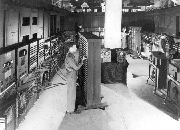
In our increasingly electronic world, microchips are the brains behind almost everything we use. So, how are semiconductors made?
What is a Semiconductor Chip?
Semiconductors are sets of electronic circuits on a small flat piece of silicon. They are the building blocks of modern digital technology, powering a wide array of devices, from smartphones and computers to cars and medical equipment. With over 1 trillion chips manufactured each year the industry continuously grows to meet needs. So, let’s take a look at how semiconductor chips are made.
How Semiconductor Manufacturing Begins
The semiconductor manufacturing process begins with sand – silicon rich sand! Silicon falls between being between an insulator and a conductor. This property enables it to be altered through a process known as doping, where impurities are added to regulate signals passing through it.
While silicon is widely available on Earth, it usually forms chemical bonds with oxygen. To separate it, sand and carbon are melted in crucibles, producing carbon monoxide and 99.9% pure silicon. Through further processing, this silicon is refined into ultra-pure silicon.
Wafer Manufacturing
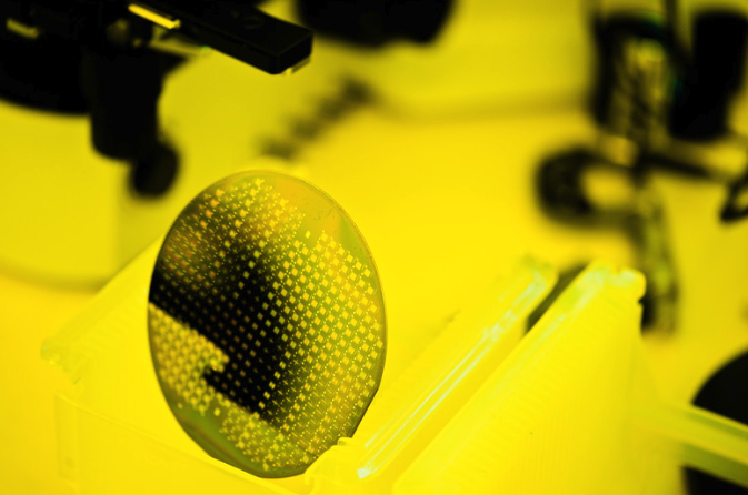
The process begins with placing a seed crystal in contact with molten silicon and slowly pulling it away. As the seed crystal is pulled away, silicon atoms adhere to its surface, forming a single crystal of pure silicon. Finally, a wafer slicer is used to cut the silicon into thin slices, ranging from 1-12 inches in diameter, and then polished to remove any impurities.
Now, semiconductor manufacturing can begin! Production commences under sterile conditions to prevent any dust contamination that could jeopardize the entire batch.
Deposition Stage
Next is the deposition stage. In this stage, a thin layer of conductive silicon dioxide is applied to the wafer’s surface to create an insulating foundation. This protective layer safeguards the silicon from oxidation and potential impurity infiltration
Oxidation
The oxidation process is a chemical reaction that occurs when silicon is exposed to oxygen. The oxygen atoms react with the silicon atoms to form silicon dioxide. The silicon dioxide layer is a very good insulator, which helps to protect the underlying silicon from damage. This is a critical step in the semiconductor manufacturing process. The silicon dioxide layer protects the underlying silicon from damage and provides a surface for the next steps of the process
Mask Stage
In the mask stage, a circuit design is generated using a computer-aided drafting machine to produce what is known as a mask. This mask consists of clear areas that function as a template on the wafer for defining patterns and structures during the photolithography process.
In the photolithography stage, a drop of a light-sensitive chemical called photo-resistant is placed in the center of the silicon wafer and spun rapidly. This distributes the photoresist over the entire surface of the wafer.
Photolithography Stage
In the photolithography stage, a drop of a light-sensitive chemical called photo-resistant is placed in the center of the silicon wafer and spun rapidly. This distributes the photoresist over the entire surface of the wafer.
The Photolithography Machine
The wafer is then put into a photolithography machine and exposed to ultraviolet light – this is the most crucial step in the semiconductor manufacturing process. The ultraviolet light passes through the transparent regions of the mask, exposing the underlying photoresist on the wafer. This exposure causes a chemical change, hardening the photoresist and embedding the circuitry pattern from the mask onto the wafer.
Because the spaces between circuits and components are so small, ultraviolet light with a very short wavelength and beams of electrons or x-rays are sometimes used to squeeze through the tiny clear areas on the mask to irradiate the photoresist.
Etching Process
The next step is to etch away the exposed silicon dioxide using a chemical or plasma etch. This leaves behind a pattern of exposed silicon, which is used to create the transistors and other components of the semiconductor. The etching process creates the desired patterns in the semiconductor material. There are two main types of etching: wet and dry.
Wet etching: Washes the wafer in a chemical bath
Dry etching: Uses gases to define the exposed pattern on the wafer
Doping
To create transistors and other electronic components, specific areas of the silicon need to be doped with impurities to alter their electrical properties.
Dopants such as phosphorus or boron are introduced in a process called diffusion (or ion implantation), defining the conductive insulating regions of the microchip.
Ion Implementation
Ion implantation is a process used to introduce impurities into the semiconductor material. This is done by bombarding the wafer with ions of the desired impurity. The impurities can be used to change the electrical properties of the semiconductor, such as its conductivity.
The ion implantation process begins with the creation of a plasma. The plasma is a gas that has been ionized. The ionized gas is then used to accelerate the ions of the desired impurity. The accelerated ions are then directed at the wafer. The ions penetrate the surface of the wafer and become embedded in the semiconductor material. The number of ions that are implanted and the depth to which they are implanted are controlled by the energy of the ions and the time that they are allowed to interact with the wafer. The ion implantation process is used to add impurities to the semiconductor wafer. The impurities can be used to change the electrical properties of the semiconductor, such as its conductivity.
After ion implementation, various materials such as metals and insulators are deposited onto the wafer’s surface using techniques like Chemical Vapor Deposition (CVD) or Physical Vapor Deposition (PVD). These deposited layers form the conductive paths and insulating layers that make up the chip’s circuitry.
Through repeated photolithography and etching steps, multiple layers of circuits can be built up to add complexity to the chips design.
Metal Wiring
The next step is to connect the different components of the semiconductor. This is done by depositing a thin layer of metal, such as copper, on the surface of the wafer. The metal is then patterned using photolithography and etched to create the desired connections. The metal wiring process is used to connect the different components of the semiconductor. The metal is deposited on the wafer using a process called electroplating. The metal is then patterned using photolithography and etched to create the desired connections.
Electrical Die Sorting
In this step, the electrical properties of the semiconductor are tested. This is done by applying a voltage to the different components and measuring the current that flows. Any semiconductors that do not meet the desired specifications are discarded. The electrical die-sorting process is used to test the electrical properties of the semiconductor. The semiconductor is tested by applying a voltage to the different components and measuring the current that flows. Any semiconductors that do not meet the desired specifications are discarded.
Testing and Packaging
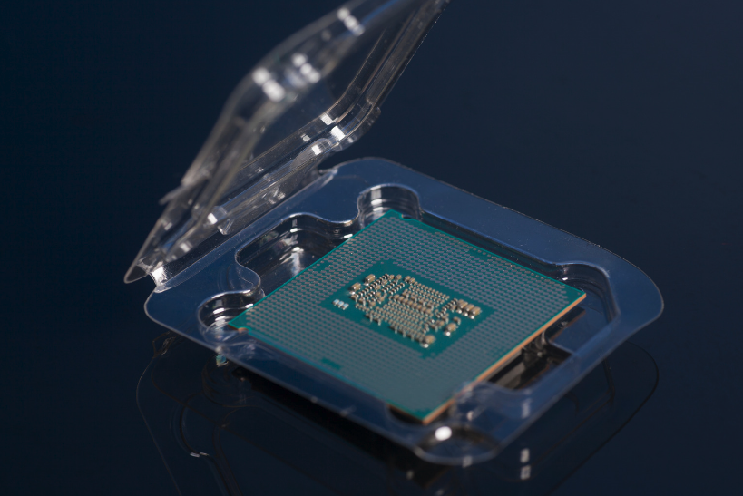
The last step in the semiconductor manufacturing process is the testing and packaging process. The wafer undergoes testing to identify and eliminate defective chips to ensure the final product’s functionality. After testing, the chips are separated and placed into protective packaging. These packages provide electrical connections and protect the chip from external elements. The packaged chips then undergo testing again to confirm they meet performance standards. This thorough testing involves evaluations and sometimes environmental tests to ensure reliability and longevity.
- The most common type of packaging is a plastic case with metal leads. The leads are used to connect the semiconductor to other components.
For an even deeper look into how microchips are made, check out this video!
The Basic Components of Semiconductor Chips
Semiconductor chips are circuits built on an incredibly small scale. This means they have a basic set of components, including capacitors, resistors and transistors.
Capacitors: Temporarily store an electrical charge
Resistors: Control the electrical current
Transistors: Amplify or switch the electrical signals passing through for highly advanced chips
Semiconductor Manufacturing from Beginning to End
From the raw material of sand to final testing, the semiconductor manufacturing process is a marvel of modern engineering. These powerful devices serve as the foundation of our most advanced technologies.
The semiconductor industry is facing a number of challenges, including the increasing cost of manufacturing, the need for more advanced manufacturing technologies, and the growing competition from China. However, the industry is also seeing a number of opportunities, such as the demand for new and more powerful semiconductors from the automotive and artificial intelligence industries. However, as the demand for chips continues to grow across various industries, chip manufacturing will only advance further. Understanding how semiconductor chips are made highlights the incredible innovation and expertise that drives our digital world forward.
Need help finding a chip? Get a quote now!

Learn more at Samsung and Nanotronics.