Introduction to the Altera MAX 10 FPGA
The MAX 10 FPGA is a high-performance, low-cost FPGA developed by Altera (now part of Intel). Built on the Arria 10 architecture, it combines performance and affordability, making it a popular choice for a wide range of applications. With features such as a scalable logic array, embedded memory blocks, DSP blocks, and high-speed transceivers, the Altera MAX 10 FPGA offers a versatile platform for digital design implementations.

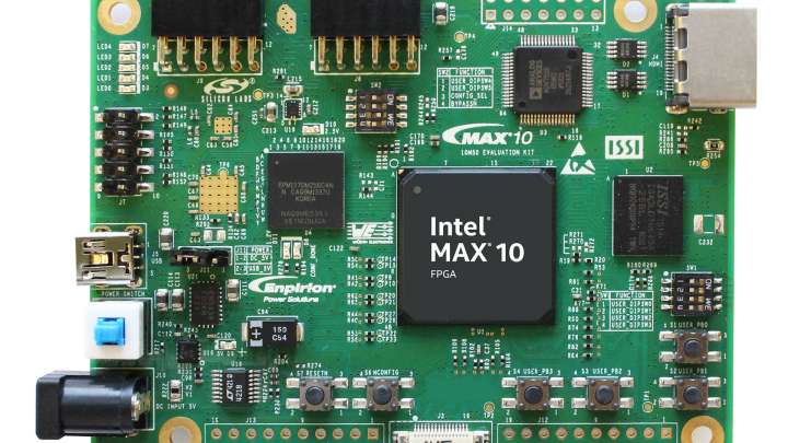
Max 10 FPGA (Image source: Intel)
MAX 10 FPGA Architecture
The Altera MAX 10 FPGA architecture is based on the Arria 10 technology, known for its high performance and low power consumption. It consists of several key components:
Scalable Logic Array: The MAX 10 FPGA provides a scalable logic array that can accommodate up to 100,000 logic cells. These logic cells can be interconnected to implement complex digital designs efficiently.
Embedded Memory Blocks: To enable efficient data storage and processing, the Altera MAX 10 FPGA includes embedded memory blocks. These blocks can provide up to 128MB of on-chip memory, allowing for high-speed access and manipulation of data.
Digital Signal Processing (DSP) Blocks: DSP blocks are specialized components within the MAX 10 FPGA that are optimized for performing high-speed arithmetic operations. These blocks are useful for implementing algorithms such as digital filters, signal processing, and mathematical computations.
High-Speed Transceivers: The MAX 10 FPGA supports high-speed transceivers, which enable fast data communication and interconnectivity. These transceivers can provide up to 100Gbps of bandwidth, making the MAX 10 FPGA suitable for applications requiring high-speed data transfer.
Altera MAX 10 FPGA Features
The MAX 10 FPGA offers several notable features that contribute to its versatility and performance:
Logic Cells: With support for up to 100,000 logic cells, the Altera MAX 10 FPGA provides ample resources for implementing complex digital designs. Logic cells are fundamental building blocks that can perform various logical operations, enabling the creation of intricate digital circuits.
On-Chip Memory: The MAX 10 FPGA includes embedded memory blocks, providing up to 128MB of on-chip memory. This on-chip memory allows for efficient data storage and processing, reducing the need for external memory components.
Transceiver Bandwidth: High-speed transceivers are integrated into the MAX 10 FPGA, offering up to 100Gbps of bandwidth. This feature enables the FPGA to handle high-speed data communication and interconnectivity, making it suitable for applications that require fast data transfer rates.
DDR4 Memory Support: The MAX 10 FPGA includes dedicated memory controllers that support DDR4 SDRAM. This support allows for efficient interfacing with DDR4 memory modules, enabling faster and more reliable memory access.
I/O Interfaces: The MAX 10 FPGA supports multiple I/O standards, including LVDS, LVCMOS, and SSTL. This flexibility enables seamless integration with various external devices and peripherals, making it easier to interface the FPGA with the rest of the system.
Altera MAX 10 FPGA Applications
The Altera MAX 10 FPGA finds applications in a diverse range of fields:
Industrial Automation: The MAX 10 FPGA can be used in industrial automation settings to implement real-time control systems, motor control, and communication interfaces. Its high-performance capabilities and flexibility make it well-suited for industrial applications that require precise control and data processing.
Medical Devices: In the field of medical devices, the Altera MAX 10 FPGA provides a flexible platform for designing and implementing various systems. It can be used in applications such as patient monitoring systems, medical imaging equipment, and diagnostic instruments, where high-performance processing and real-time data analysis are crucial.
Networking: The MAX 10 FPGA is an excellent choice for networking applications that require high-bandwidth and low-latency data processing. It can be used to develop routers, switches, network interface cards (NICs), and other networking equipment. The FPGA’s ability to handle high-speed data communication and its support for various I/O standards make it ideal for networking applications.
Consumer Electronics: The Altera MAX 10 FPGA is well-suited for consumer electronics products that demand high-performance and customization. It can be used in applications such as high-definition displays, audio/video processing devices, smart home automation systems, and other consumer electronics where flexibility, speed, and power efficiency are essential.
Test and Measurement: The MAX 10 FPGA is also suitable for test and measurement applications. Its programmable nature allows for the implementation of signal processing algorithms, data acquisition, and instrument control. It can be utilized in test and measurement equipment, such as oscilloscopes, spectrum analyzers, and data loggers.
MAX 10 FPGA Programming
Programming the Altera MAX 10 FPGA involves using design tools provided by Intel, specifically the Quartus Prime software suite. Quartus Prime offers a comprehensive set of tools for designing, implementing, and programming the MAX 10 FPGA. The software suite supports various programming languages, including VHDL and Verilog, which are widely used in digital design.
The programming process typically involves the following steps:
Design Entry: The design entry stage involves describing the digital design using a hardware description language (HDL) such as VHDL or Verilog. Designers define the desired functionality and structure of the FPGA design in this step.
Compilation and Synthesis: After the design entry, the Quartus Prime software compiles and synthesizes the design description into a netlist, which represents the interconnections and functionality of the design. The software optimizes the design to maximize performance and resource utilization.
Place and Route: In this step, the software determines the optimal physical placement of the design components on the FPGA chip and routes the interconnections between them. This process ensures that the design meets timing requirements and minimizes signal delays.
Configuration Generation: Once the design is placed and routed, the Quartus Prime software generates a configuration file that contains the programming data for the Altera MAX 10 FPGA. This file specifies how the FPGA resources should be initialized and connected to implement the desired functionality.
Programming the MAX 10 FPGA: The final step involves transferring the configuration file to the MAX 10 FPGA. This can be done using various methods, such as using a programmer device connected to the FPGA’s programming interface or configuring the FPGA from an on-board configuration memory.
The Quartus Prime software suite provides a user-friendly interface for managing the programming process and offers advanced features for debugging and verifying the FPGA design before programming it onto the MAX 10 FPGA.
Altera MAX 10 FPGA Tools
To facilitate the development and programming of the MAX 10 FPGA, Intel provides a range of tools and resources:
Quartus Prime: The Quartus Prime software suite is the primary tool for designing, implementing, and programming the Altera MAX 10 FPGA. It includes a design entry environment, synthesis and optimization tools, simulation capabilities, and a programming interface.
ModelSim: ModelSim is a widely used simulator that integrates with Quartus Prime. It allows designers to verify and debug their digital designs before programming them onto the MAX 10 FPGA. ModelSim provides a comprehensive set of simulation features and supports various design languages, including VHDL and Verilog.
Intel FPGA IP Library: Intel provides a library of pre-designed intellectual property (IP) cores that can be used in Altera MAX 10 FPGA designs. These IP cores are pre-verified and offer ready-to-use functionality, allowing designers to save time and effort in implementing common features.
Design Examples and Application Notes: Intel offers a collection of design examples and application notes that demonstrate the implementation of various functionalities and applications using the MAX 10 FPGA. These resources provide practical insights, guidelines, and code snippets that can assist designers in leveraging the features and capabilities of the MAX 10 FPGA.
MAX 10 FPGA Development Kit: Intel offers a MAX 10 FPGA development kit that provides a complete hardware and software platform for developing and testing FPGA designs. The development kit includes the necessary hardware board, documentation, and example projects to help designers get started quickly.
Online Forums and Communities: Intel hosts online forums and communities where FPGA developers can connect, share knowledge, seek assistance, and exchange ideas related to the Altera MAX 10 FPGA. These platforms provide a valuable resource for developers to interact with peers, discuss challenges, and gain insights from experienced FPGA enthusiasts.
Empowering Innovation with Versatile and Accessible Solutions
The MAX 10 FPGA from Altera is a powerful and cost-effective FPGA solution that offers a wide range of features and capabilities. Its architecture, extensive logic capacity, on-chip memory, transceiver bandwidth, and support for various I/O standards make it suitable for diverse applications in industrial automation, medical devices, networking, consumer electronics, and test and measurement.
The Quartus Prime software suite and tools like ModelSim provide a comprehensive platform for designing, programming, and simulating MAX 10 FPGA-based solutions. The availability of resources such as user manuals, forums, design examples, and training materials further supports developers throughout their FPGA development journey.
With its versatility and accessibility, the MAX 10 FPGA empowers developers to create innovative and efficient solutions for various applications. Whether you are an experienced FPGA developer or new to the field, the Altera MAX 10 FPGA offers ample resources and support to bring your ideas to life.
Contact us today for comprehensive support and to source your FPGA and electronic component needs!


